温馨提醒:图片仅供参考,商品以实物为准
 数据手册
数据手册
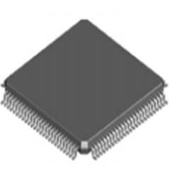
自营 HB8513F
- 库存
- 0 个
- 样片库存
- 0 个
- 起订
- >= 1 个
- 交期
- 订货交期以实际为准
- 仓库
- 境内
- 数量
- X ¥0(单价)
- 合计:


深圳市浩博高科技有限公司 2/28 V1.0.6
HB8513F Datasheet 浩博高科技
Table of Contents 1 Features ........................................................................................................... 3
1.1 Application Field ................................................................................................................ 3 2 General Description ......................................................................................... 4 3 Pin Configurations ............................................................................................ 5
3.1 Pad Assignment .................................................................................. 3.2 Pin Description .................................................................................................................. 6
4 Block Diagram .................................................................................................. 7 5 Function Description ........................................................................................ 8
5.1 Registers ........................................................................................................................... 8 5.2 Accumulator ...................................................................................................................... 8 5.3 Index Register(X,Y) ........................................................................................................... 8 5.4 Processor Status Register ................................................................................................. 8 5.5 Program Counter(PC) ....................................................................................................... 8 5.6 Stack Point(S) ................................................................................................................... 8
6 Memory Organization ....................................................................................... 9 6.1 SFR Mapping .................................................................................................................. 10 6.2 Write Protect Function Register ....................................................................................... 11 6.3 IAP Write Protect Register ............................................................................................... 11
7 Interrupt.......................................................................................................... 12 7.1 Interrupt Register ............................................................................................................. 12 7.2 Interrupt System .............................................................................................................. 13
8 Reset ............................................................................................................. 14 8.1 Low Voltage Reset (LVR) ................................................................................................ 14 8.2 Watchdog Timer (WDT) ................................................................................................... 15 8.3 Reset OK......................................................................................................................... 15
9 Power Control ................................................................................................ 16 9.1 Power Control Register ................................................................................................... 16
10 Divider ....................................................................................................... 17 10.1 Divider ............................................................................................................................. 17
11 Timer ......................................................................................................... 18 11.1 Timer0 ............................................................................................................................. 18 11.2 Timer1 ............................................................................................................................. 19
12 Configurable I/O Ports ............................................................................... 20 12.1 Port 0 .............................................................................................................................. 20 12.2 Port 1 .............................................................................................................................. 21 12.3 Port 2 .............................................................................................................................. 21 12.4 High sink output............................................................................................................... 22
13 LCD Controller/Driver ................................................................................ 23 14 Option Register ......................................................................................... 25 15 Application Circuit ..................................................................................... 26 16 Electrical Characteristics ........................................................................... 27
16.1 Absolute Maximum Rating ............................................................................................... 27 16.2 DC Characteristics .......................................................................................................... 27 16.3 AC Characteristics ........................................................................................................... 28
- 数据手册